(C)2006-2008 Miguel Angel Rodríguez Jódar. Grupo de Robótica y Tecnología de los Computadores aplicada a la Rehabilitación. Dept. Arquitectura y Tecnología de Computadores. Universidad de Sevilla.

This work is licensed under a
Creative Commons lincense. As the author, I reserve the right to change the license of this document.
DECRIPTION AND MAKING-OF
After experimenting some time with an alternative to rebuild a rubber-version Spectrum keyboard membrane from scratch, I wanted to do the same with the Plus membrane. The philosophy is the same, but the making was too hard: the Plus membrane has not two, but four circuits and two inner layers to isolate them. This is necesary to be able to simulate the closing of two independent circuits with a single push.
The Plus cabinet has enough room, at both sides, to fit small PCB's. Besides, the cabinet can be drilled to expose connectors to the outside. I took some measures and went to one of my department labs to take two microcontroller trainers: one from Microchip and another one from Silicon Labs.
At first I were intented to use Micrchip's as the PIC is very popular in Spain. However, after taking a closer look at Silicon Labs specifications, I realize there was no place for comparisons: Silicon Labs medium-low class chips are almost equivalent to high-class PIC's. Low class Silicon Labs microcontrollers start with 12 MHz clock and high class reach 100 MHz.. Besides, the IDE and debugging facilities, with no waste of internal resources on the chip during debug sessions, and above all, the fact that many people in my lab were using the Silicon Labs chip and encouraged me to use it instead of Microchip's, helped me to take my final decision.
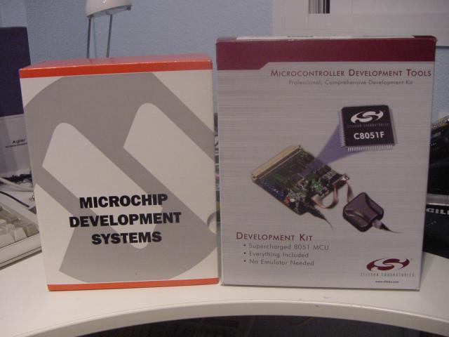
Microchip's trainer contents .
Silicon Labs trainer contents
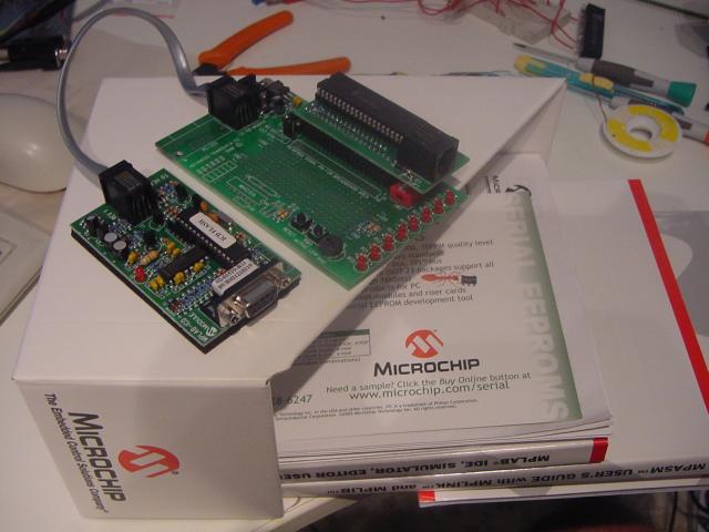
Another thing in favour of Silicon Labs is one leaflet, that you can see in the photo, behind the install CD, were you are guided in a few steps from nothing, to have a complete program up and running in less than five minutes. I learnt the basics of this MCU very quickly.
Thus, the proposed interface is based on a model C8051F343 microcontroller from Silicon Labs, although the PCB is compatible with another one, the C8051F320. Both are 8051-core based, with 25 I/O lines, USB slave interface (which we will not use), and support for SPI, UART, timers, etc.. They work at 3.3 V, which makes it very suitable for interfacing with memories SD / MMC, and yet can manage TTL levels. The difference between the two is that the F343 can reach 48 MHz clock frequency, and has 4KB of XRAM, and the F320 reaches 25 MHz with 2KB of XRAM. The firmware written for this microcontroller uses only 256 bytes of XRAM, and a few positions of direct RAM. They have a built-in oscillator, so does not need quartz crystal to work at 25 or 48 MHz. In fact, the final design there's only one active component, the microcontroller, being the rest resistors and capacitors.
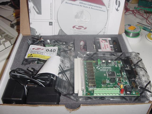
The Silicon Labs development kit I was using to the date is based on a CAN bus enabled chip, which I don't use. The IDE allows assembler and C. Assuming I would have to deal with precisse timings, I chose assembler, and a home-made devkit based upon the F320.
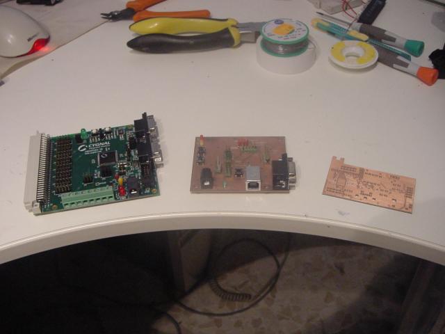
Original development kit ,featuring theF040 (bus CAN), home-made F320 dev kit, and PCB for the keyboard interface, with the F343.
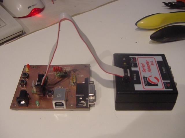
C8051F320 devkit and JTAG adapter, for program downloading and debugging.
One of the advantages of F320 (and of F343 since both have the same pinout) is still being a 3.3 V device, they don't need a external voltage regulator to get it working. Instead, they can be fed with 5V, converting to 3.3V internally. This is because these micros are designed to be used in USB applications, which gives 5V over the USB wire to feed the device. The devkit used in the initial tests, in fact, is fed from the PC with a USB cable, which only used two pins for supply.
First prototype. Note that there are only three lines that are used in the connector back Spectrum: 5V, ground, and the reset signal, we use because the uC has the ability to reset the Spectrum from the keyboard (yes, yes, with Control-Alt - Delete: D)
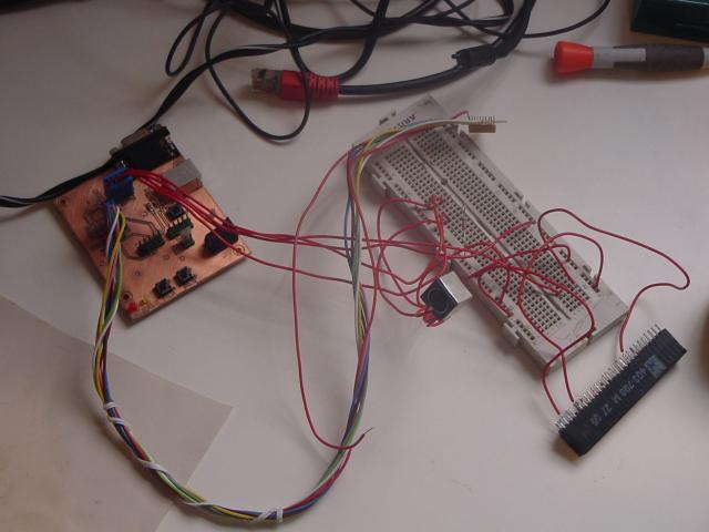
Prior to the F343, and with the false asumption that the F320 would not be fast enough, I considered using the F352, which is somewhat faster than the F343 and with enough XRAM, but has two disadvantages: it only has 17 I/O pins, and it needs an external regulator. I even made a PCB for this uC, but couting with the F343, the whole thing becomes easier (and cheaper).
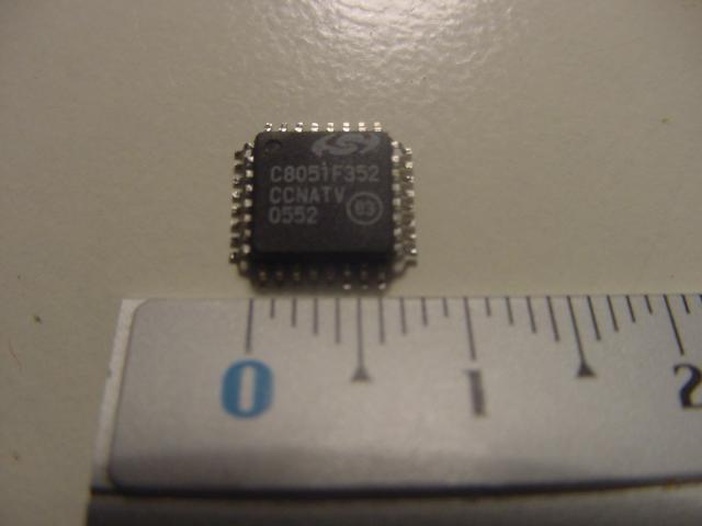
Silicon Labs C8051F352.
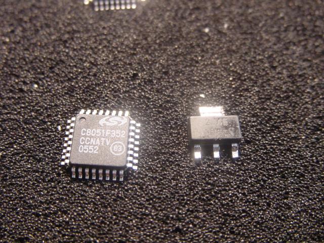
F352 and the SIMD 3.3V external regulator.
This is the schematic for the F343 version. The amazing thing is that you do not need anything else, just the uC and a few additional components: a small RC cricuit for the reset and the JTAG interface, filter capacitors, and pull-up resistors to the keyboard lines and ZX Spectrum address lines (half-rows).
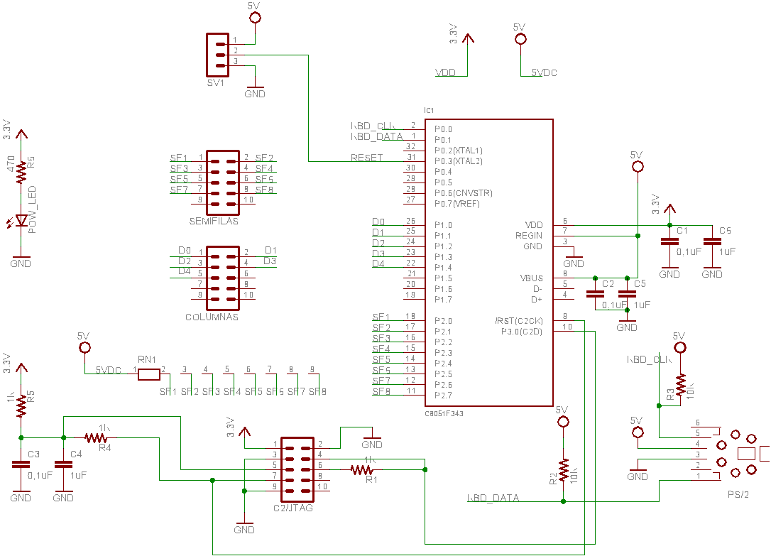
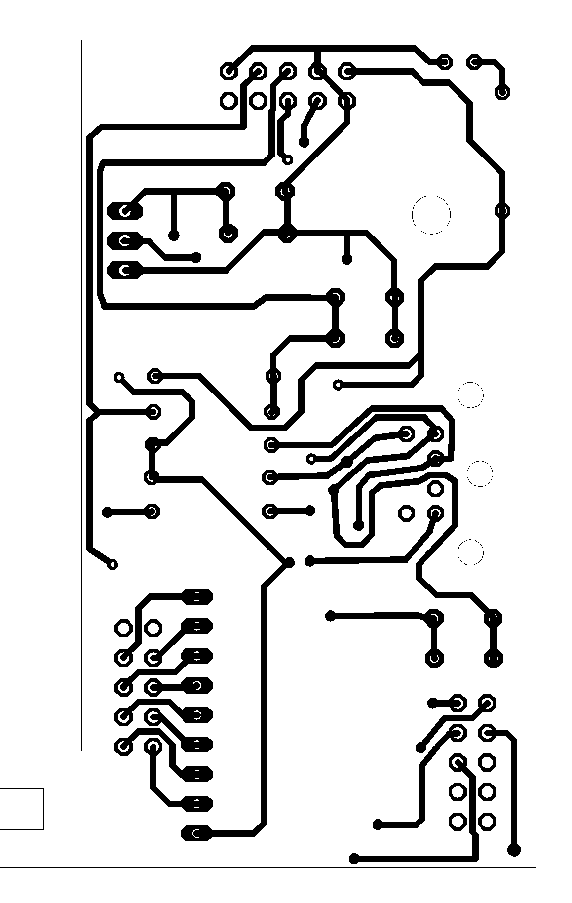
Schematic (clic to zoom)
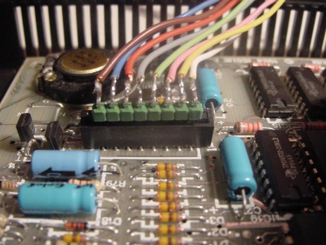
Half-row lines are configured as open collector pins (8 pin header), and data as push-pull pins (5 pin header). SV1 carries the three signals you have to wire on the ZX Spectrum PCB: 5V, ground and reset, the latter optional, only if you want to use the reset keyboard.
The half-row lines go directly to the port 2 of 8051, and the column lines go to port 1. Port 0 is left to control signals, in this case, the two signals needed by the keyboard (clock and data) and an output signal directly to the Z80 reset pin. Clock signal go to one interrupt pin. The firmware in the 8051 ties an interrupt service routine, so it's run whenever a falling edge happens on clock line, reading one data bit everytime the interrupt service routine is invoked. The 8051 provides SPI, but the data format is not compatible with that used by the keyboard.
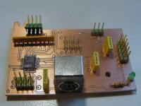
As it's time to build the board, it may seem difficult to solder the microcontroller, which is a 32 pin QFP device. Actually it's not that hard, and it only requires a thin solder tip (1 mm). This is how the uC looks like one it is solded to the PCB.
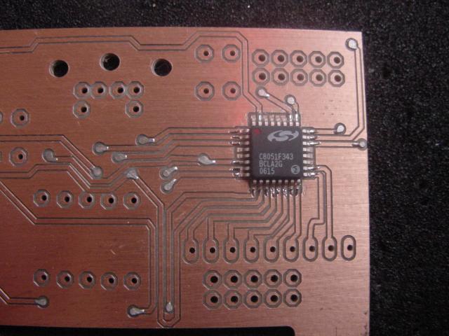
The PCB almost completely populated:
It has two holes so you can screw the PCB to the Spectrum casing. One of them matches a mouting hole present in the Spectrum+ casing, that is not in use. The other one is not really a hole. It fits a screw present in the Spectrum+, near the loudspeaker. Simply raise that screw and use it to prevent the PCB from moving inwards when you push it while you plug-in the PS/2 keyboard.
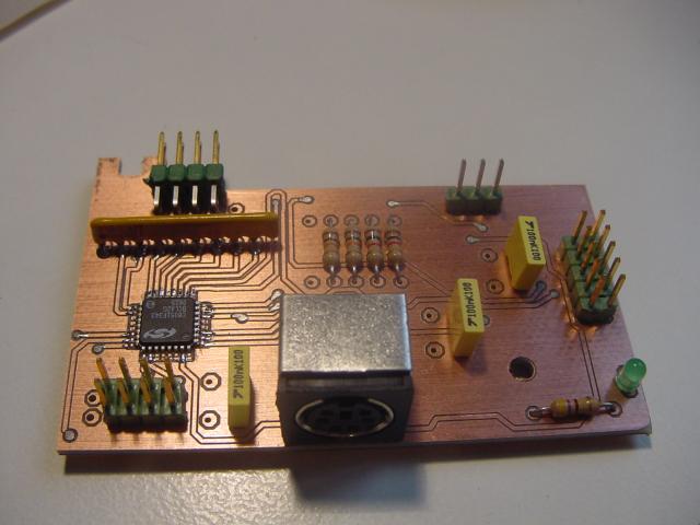
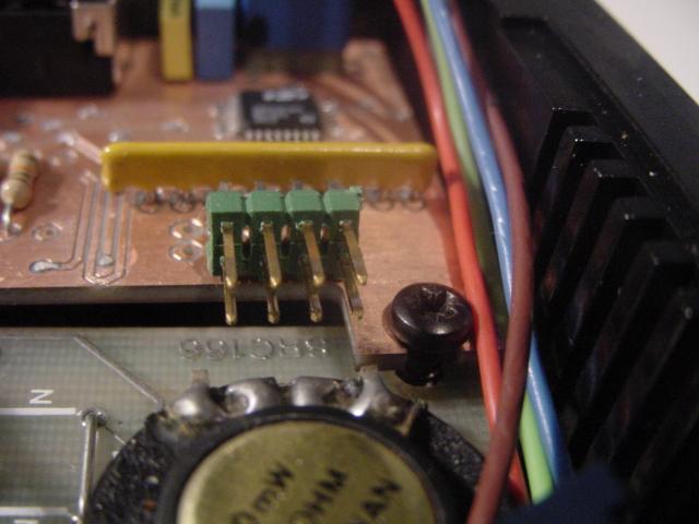
Deail showing one of the mounting screws, power LED, JTAG connector, and the three pins of SV1 connector (from top to bottom: +5V, RESET, GND)
Detail showing the screw near the loudspeaker, which has been raised a little to fit the adapter PCB and prevent it to move.
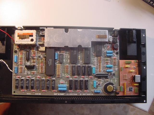
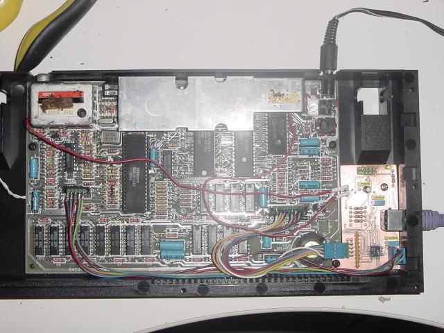
Once it's mounted at the right side of the case:
The 8 pin header at the side of the loudspeaker is tilted slightly upwards, so the connector with the 8 wires from the Spectrum doesn't clash with the speaker.
The other end of the column and half-row cables is a piece of strip pin.
So you can "plug" the strip on the correspoding keyboard connector at the Spectrum side.
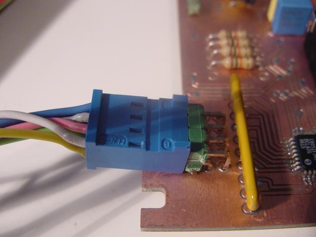
Using the SV1 pins, we take power and ground to the adapter. At the right side we'll make a hole to reach the PS/2 connector from the outside.
It was easy to make the hole for the PS/2 connector, as the Spectrum+ case has a circle serigraphied at the same distance the hole has to be opened.
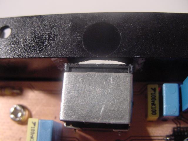
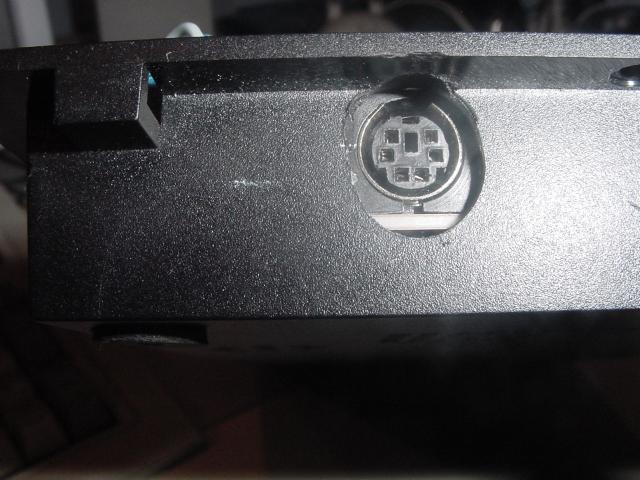
The hole for the PS/2 connector is wider than the connector itself because some PS/2 jacks have a wider handle.
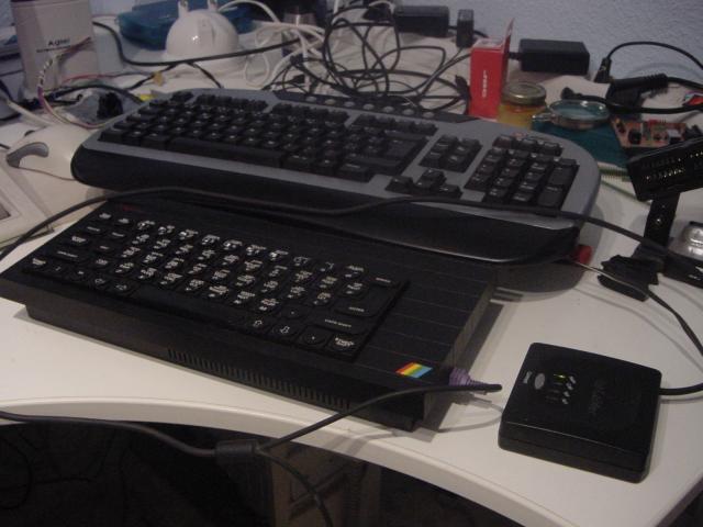
Once it's programmed, the JTAG is of not use. We can freely close the Spectrum case and forget forever about the keyboard. Here you have it, with a wireless keyboard from Labtec.
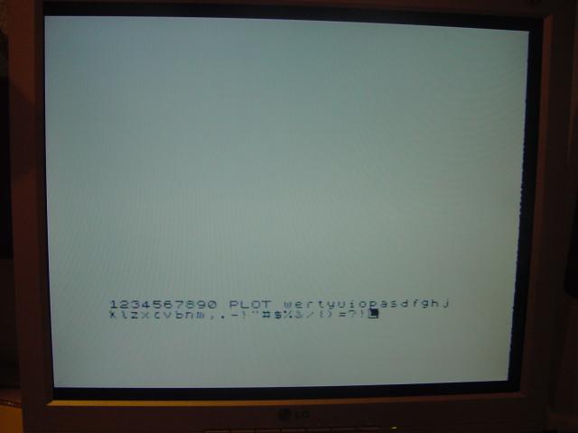
For the next snapshot, these keys were typed at the wireless keyboard in sequence: 1 2 3 4 5 6 7 8 9 0 Q W E R T Y U I O P A S D F G H J K L Z X C V B N M , . - following the number keys (at the top of the keyboard) with shift pressed: ! " · (giving #) $ % & / ( ) = ? ¿ (giving !). This example comes from a spanish keyboard.
MODO DE OPERACION
Al encender el Spectrum con el teclado, el microcontrolador lo resetea y para indicar que todo ha ido bien, deja encendida la luz de Bloq Num. A partir de ese momento, el teclado está listo para ser usado.
- Se reconocen todas las teclas alfabéticas.
- Las dos teclas de mayúsculas aplicadas sobre una tecla alfabética dan el mismo caracter en mayúsculas, aplicadas sobre un número u otra tecla del bloque de teclado principal, dan el carácter que tengan serigrafiado.
- Se usa el modelo de teclado español de 101/102 teclas.
- Las teclas del cursor están mapeadas a las propias del Spectrum (ej: cursor abajo corresponde a CAPS SHIFT + 6)
- La tecla ESC corresponde a CAPS SHIFT + SPACE
- La tecla de Bloq. Mayús corresponde a CAPS SHIFT + 2
- La tecla Alt Gr corresponde a CAPS SHIFT + 9 (modo G en el Spectrum)
- La tecla F2 (tecla de edición en muchas aplicaciones de Windows) corresponde a CAPS SHIFT + 1 (EDIT en el Spectrum)
- El tabulador corresponde a CAPS SHIFT + SYMBOL SHIFT (modo E en el Spectrum)
- La tecla Backspace (borrar) es CAPS SHIFT + 0 (DELETE en el Spectrum)
- Control izquierda está mapeada a CAPS SHIFT y Control derecha a SYMBOL SHIFT.
- El bloque numérico se comporta como si siempre estuviera activado el bloqueo numérico, esto es, no se emulan cursores en este bloque.
- La tecla Bloq Despl activa/desactiva la conmutación entre el modo cursores (el normal) y el modo joystick Sinclair. En este modo, el indicar Bloq Despl se enciende y las teclas del cursor pasan a ser las correspondientes direcciones en un joystick norma Sinclair. Cualquiera de las dos teclas de Control actúan como disparo (para asemejar un poco a cómo están dispuestas estas mismas teclas en el MAME).
- Por último, si la línea de reset está conectada desde nuestra placa hacia el Spectrum, la combinación Ctrl-Alt-Supr provoca que el microcontrolador dispare un pulso bajo de unos 200 microsegundos en la línea de reset, permitiendo así reiniciar el Spectrum desde el teclado.
PROGRAMA INTERNO DEL MICROCONTROLADOR
Esta sección aún no está documentada. La razón fundamental es que quiero pulir un poco más el programa y añadirle algunas funciones que me parecen interesantes. Entre las cosas a pulir, la más importante es soportar el scan mode 2, que es el más habitual. Ahora mismo sólo se soporta el scan mode 3, que es el más fácil de depurar. Entre las cosas menos importantes, hacer más robusta la función de enviar comandos al teclado y un fallejo intermitente cuando se conmuta de modo joystick a modo normal.
Entre las cosas a añadir, pues la que tengo ahora en mente es la posibilidad de grabar y reproducir macros de teclado, que el propio programa almacenaría en flash para que no se pierdan cuando el micro se apague. De esa forma, podemos tener comandos directos, tales como LOAD "gens3" CODE 26000: RANDOMIZE USR 26000 en una sola tecla, o incluso pequeños programas escritos en BASIC, que el microcontrolador teclearía por nosotros.
De todas formas, para los impacientes, se suministra la versión actual del programa, con las limitaciones expuestas.
Hay un detalle técnico que tiene que ver con un comportamiento de la ULA que no conocía, que ha condicionado en buena medida el diseño del firmware. Lo comentaré en breve.
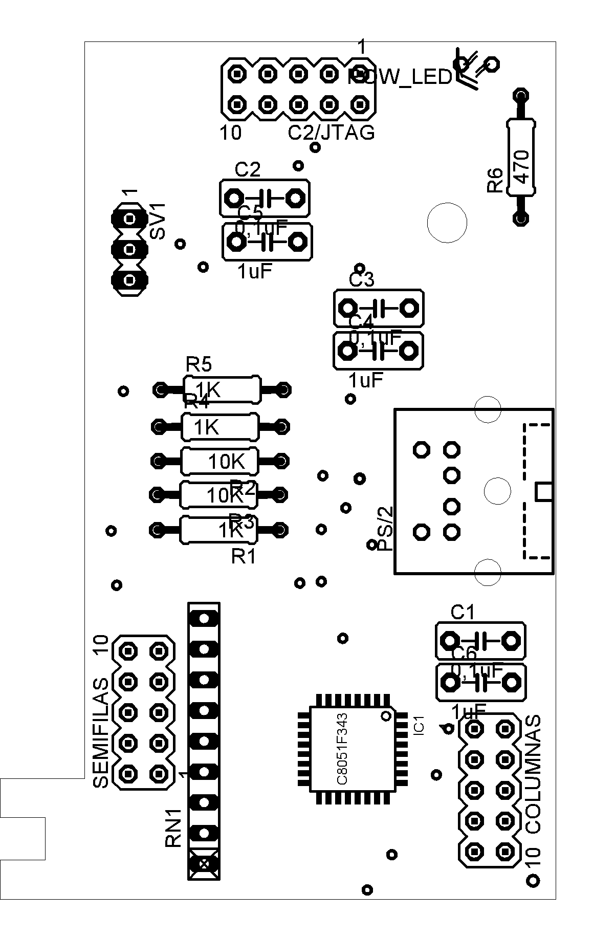
LISTA DE MATERIALES Y COSTE ESTIMADO
Parte |
Nombre |
Notas |
| IC1 | C8051F343 | 1/4 W. También vale el C8051F320. En ese caso, soldar R1 |
| R1 | 1K | 1/4 W. No necesario para el F343. |
| R2 | 10K | 1/4 W |
| R3 | 10K | 1/4 W |
| R4 | 1K | 1/4 W |
| R5 | 1K | 1/4 W |
| R6 | 470 ohm. | 1/4 W |
| C1 | 100 nF | Poliester |
| C2 | 100 nF | Poliester |
| C3 | 100 nF | Poliester |
| C4 | 1 uF | Poliester o tántalo |
| C5 | 1 uF | Poliester, tántalo o electrolítico |
| C6 | 1 uF | Poliester o tántalo |
| RN1 | Red de resistencias 4,7K | Equivalente a 8 resistencias de 4,7K unidas entre sí por uno de sus bornes. |
| PS/2 | Conector hembra mini DIN 6 pin PCB | |
| SV1 | Conector tiras de pines acodado | 3 pines |
| SEMIFILAS | Conector tira doble de pines acodados | 4+4 pines (en la placa hay dos pines sin soldar) |
| COLUMNAS | Conector tira doble de pines vertical | 4+4 pines (de los 8 sólo se usan en realidad 5. Hay dos pines sin soldar en la placa) |
| POW_LED | LED miniatura 2mm | Color al gusto de cada uno (total, no se va a ver una vez montado todo) |
| Conector semifilas | HDC 4x2 pines, hembra | Conector hembra desde el Spectrum hasta la placa (semifilas) |
| Conector datos | HDC 4x2 pines, hembra | Conector hembra desde el Spectrum hasta la placa (datos o columnas) |
El C8051F343 sale por $7,79 y se puede pedir directamente desde Mouser Electronics, a través de la página web de Silicon Labs. Los gastos de envío salen por unos $10,70 enviando por USPS, que es lo más barato. Llega a España en unos 5-6 días laborales.
Una PCB del tamaño y disposición como la presentada aquí, sale en Futurlec por unos 7€ aproximadamente, dependiendo de si se incluye máscara de soldadura, serigrafía, etc. sale más caro. Si se la hace uno mismo, pues ya el coste estará en función de más factores.
El resto de componentes son muy baratos. Quizás entre todos no lleguen ni a 6-7€. En total, el coste en componentes y placa ronda los 20-25€, que viene a ser además el precio que se pide hoy día por una membrana de Spectrum Plus en eBay. Hay cosas como las placas o los microcontroladores, que si se piden en cantidades, sale más barata la unidad al repartirse los gastos de envío. A modo de ejemplo, 4 microcontroladores C8051F343 costaron, gastos de envío incluidos, $41,86. Cada microcontrolador salió por tanto por $10,46, que vienen a ser 8,26€.
ARCHIVOS
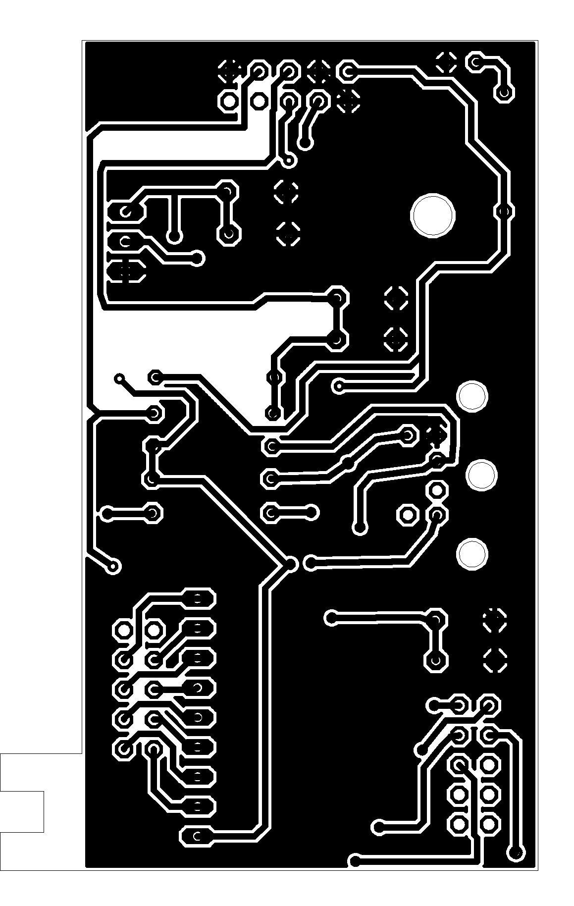
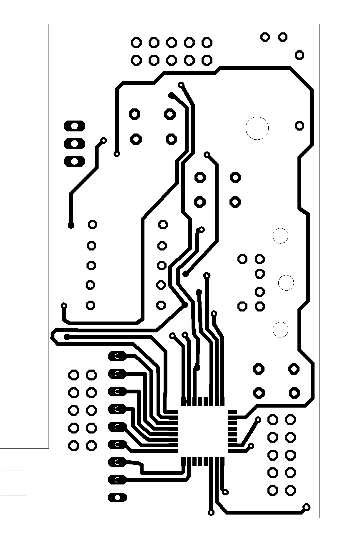
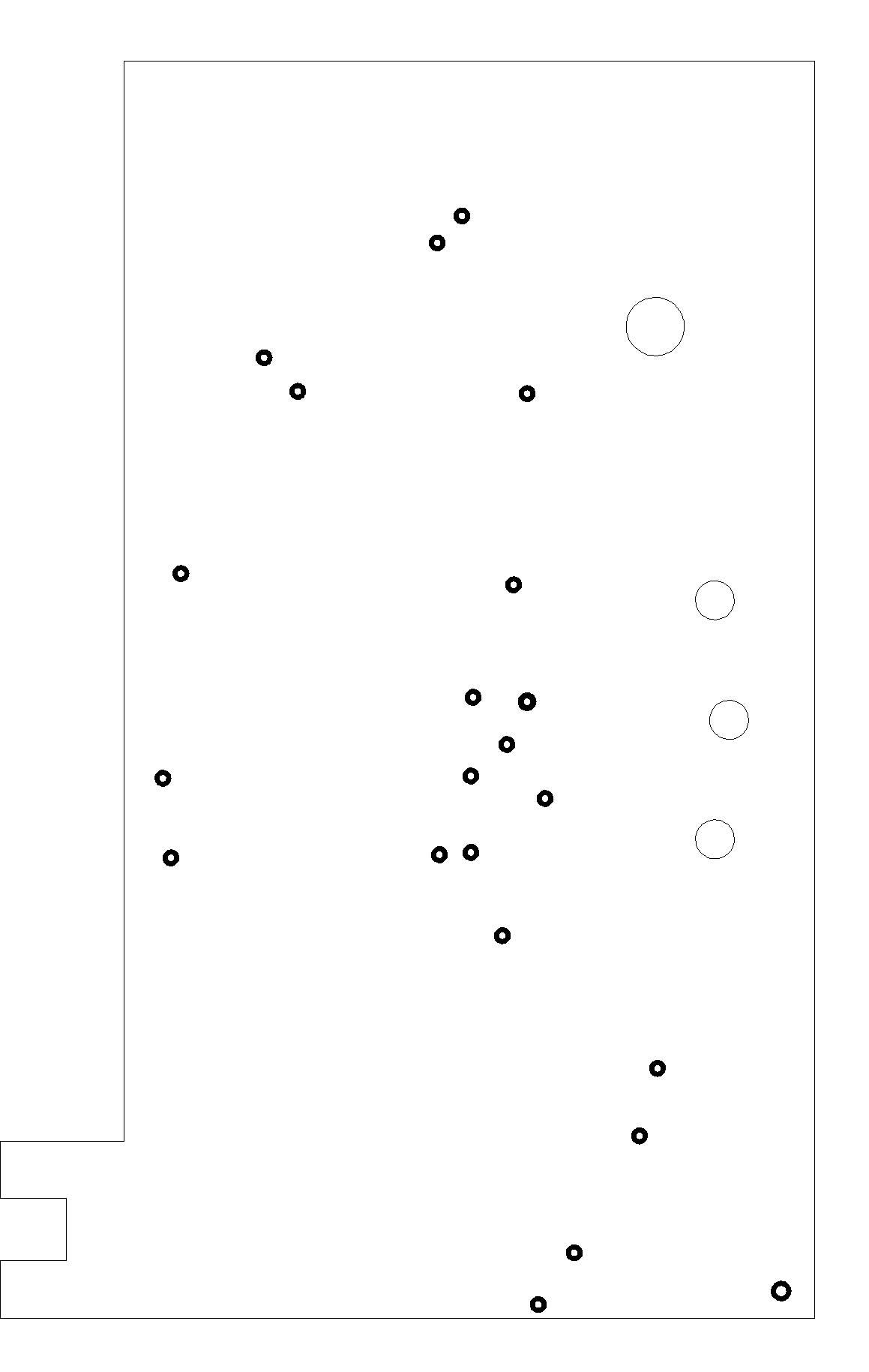
| Esquemático, placa PCB y librería con componentes de Silicon Labs, para Eagle (NOTA: la PCB aquí está sin planos de masa) | Descargar |
| Esquemático en formato PNG, alta resolución | Ver / Descargar |
| Fotolito placa, cara de pistas, sin plano de masa (PNG, 600 dpi) | Ver / Descargar |
| Fotolito placa, cara de pistas, sin plano de masa (PNG, 600 dpi) | Ver / Descargar |
| Fotolito placa, cara de componentes, sin plano de masa (PNG, 600 dpi) | Ver / Descargar |
| Fotolito placa, cara de componentes, con plano de masa (PNG, 600 dpi) | Ver / Descargar |
| Mapa de posición de componentes | Ver / Descargar |
| Mapa de posición de vías | Ver / Descargar |
| Fuente del firmware residente en el F343, v1.1 | Descargar |
| Fuente del firmware residente en el F343, v1.0 | Descargar |
HISTORICO DE CAMBIOS
- 11/10/2006. Se soporta scan mode 2 y scan mode 3. Primera versión con soporte de macros de teclado. Versión 1.1 del firmware.
- 26/09/2006. Primera puesta en público. Versión para F343. Se soporta sólo scan mode 3. Versión 1.0 del firmware.
OTROS ADAPTADORES DE TECLADO PARA SPECTRUM
- IMAR-3 (de "Droy", del Trastero del Spectrum). Descripción completa, y todo lo que se necesita para construir uno.
- Proface AT (externo). Comercializado por Sintech (¿dónde se enchufa el teclado aquí?).
- Proface AT (interno). Comercializado por Sintech (¿lo llaman interno porque está metido en una caja?).
ENLACES DE INTERES
Los he ido recopilando a medida que me ha hecho falta tal o cual información para desarrollar este proyecto.
- El bus de expansión del Spectrum. Me vinieron muy bien estos digramas para la primera versión del prototipo, que cogía las señales del bus de expansión. Artículo cortesía del Trastero del Spectrum.
- The PS/2 keyboard interface. Pues eso, todo lo que necesitaba saber acerca de la interfaz del teclado.
- El juego de instrucciones del 8051. En los datasheets de Silicon Labs sólo viene el nombre de la instrucción y los ciclos que tarda. En esta pagina comentan un poco "de qué va" cada instrucción.
- Registro de teclados de IBM. Completísimo catálogo de "layouts" de teclados de todas las nacinalidades que fueron normalizados en su día por IBM.
- Datasheet y guía de usuario del C8051F343. Disponible en la web de Silicon Labs.
- IDE y Configuration Wizard de Silicon Labs. IDE muy completo que permite trabajar en ensamblador y/o C, más una utilidad que permite mediante asistentes, generar código en C o ensamblador para programar en el micro una configuración determinada de puertos, osciladores, timers, interrupciones, etc...
AGRADECIMIENTOS
A todos mis compañeros del grupo de investigación y en especial a:
- Rafa y Claudio: por sugerirme el C8051 sobre el PIC y picarme en el tema de los microcontroladores.
- Miguel Gutierrez (tocayo y paisano): por enseñarme a usar la fresadora de circuitos impresos y enseñarme a soldar (y des-soldar) componentes SMD
- Angel, Carlos y Ramón: por todos sus buenos consejos para mejorar el invento y sobre todo, por aguantar el ruidazo del compresor de la fresadora en horas de trabajo.
- Gabriel: por lo mismo, por sus consejos a la hora de arreglar los fallejos de las primeras versiones del circuito.
A todo es.comp.sistemas.sinclair, ya que esto es esencialmente, para vosotros, para los que mantienen viva la "escene" del Spectrum.
CONTACTO
Por e-mail a la dirección: rodriguj@atc.us.es poniendo en el asunto "Sobre el adaptador PS/2 para Spectrum"